

The Application of Ceramic Substrates in MEMS Packaging
Micro-Electro-Mechanical Systems (MEMS) are at the heart of modern sensors, actuators, and miniature systems. Their packaging is not merely an enclosure; it is a critical functional component that ensures signal integrity, environmental protection, and reliable thermal management. Ceramic substrates have become the foundation of high-performance MEMS packaging due to their unique combination of excellent electrical insulation, high mechanical strength, good thermal conductivity, and resistance to harsh environments. This article explores how different ceramic materials meet the diverse and stringent demands of MEMS packaging across industries.
Why Ceramics Are Indispensable for Advanced MEMS Packaging
MEMS devices often contain delicate micromechanical structures and sensitive electronics. The packaging substrate must provide:
- A Stable, Hermetic Platform: To protect against moisture, particles, and corrosive gases.
- Effective Thermal Management: To dissipate heat from integrated ASICs or high-power elements.
- Reliable Electrical Interconnection: Supporting fine-pitch wire bonding or flip-chip attach with high electrical insulation.
- Mechanical Robustness: Withstanding handling, vibration, and thermal stresses without warping or cracking.
Ceramics inherently meet these needs, offering properties superior to organic laminates in demanding applications.
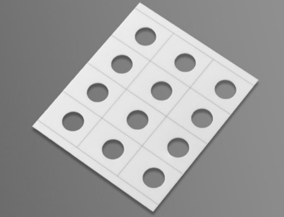
Material Selection Guide for MEMS Packaging Substrates
The optimal choice depends on the primary technical driver of your MEMS application: cost-performance balance, extreme heat dissipation, or unmatched mechanical durability.
Alumina (Al₂O₃) Ceramics: The Versatile, Cost-Effective Standard
96% Al2O3 ceramic substrates are the most widely used in MEMS. They offer a reliable balance of:
- Good Thermal Conductivity (20-30 W/m·K): Sufficient for many sensor and consumer MEMS devices.
- Excellent Electrical Insulation & High Mechanical Strength: Protects circuits and supports delicate structures.
- Superior Surface Finish: Enables precision patterning of thin-film or thick-film metallization for interconnects.
Puwei's 96 Alumina Ceramic Substrate is ideal for thick-film ceramic substrates in automotive pressure sensors, inertial measurement units (IMUs), and microfluidic devices. As a foundational Alumina Ceramics solution, it provides proven reliability.
Aluminum Nitride (AlN) Ceramics: For High-Power & Thermal-Critical MEMS
When heat is the primary constraint, AlN is the superior choice. Its high thermal conductivity (170-200 W/m·K) and closely matched coefficient of thermal expansion (CTE) to silicon make it perfect for:
- RF MEMS switches and filters generating significant heat.
- High-power optical MEMS (MOEMS) and laser systems.
- Packages integrating power management ICs alongside MEMS sensors.
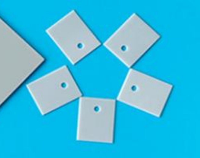
The material's low dielectric loss also benefits high-frequency MEMS applications in communications.
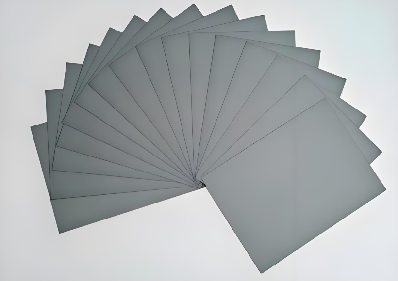
Silicon Nitride (Si₃N₄) Ceramics: The Ultimate in Durability
For MEMS operating under extreme mechanical or thermal shock, Si₃N₄ offers unmatched toughness and thermal stability.
- Exceptional Fracture Toughness: Ideal for MEMS in high-vibration environments (e.g., industrial, aerospace).
- Excellent Thermal Shock Resistance: Withstands rapid temperature cycling without failure.
- Good Chemical Inertness: Suitable for biomedical or corrosive environment MEMS sensors.
Key Considerations for MEMS Package Design with Ceramics
Collaborating with your ceramic substrate supplier early is crucial. Key steps include:
- Define Requirements: Clearly specify operating temperature range, power dissipation, hermeticity level (e.g., MIL-STD), and required I/O density.
- Select Material & Metallization: Choose the ceramic based on thermal/mechanical needs. Specify the metallization scheme (e.g., Au, Pt-Au, Ti/Ni/Ag) for bonding and sealing.
- Design for Manufacturability (DFM): Work with the manufacturer (like Puwei) on feature sizes, via placement, and tolerance to ensure a high-yield, reliable custom ceramic substrate.
- Prototype & Test: Build and rigorously test prototypes for thermal cycling, mechanical shock, and long-term reliability.
FAQ: Ceramic Substrates in MEMS Packaging
Q: Can ceramic substrates be used for wafer-level MEMS packaging?
A: Yes. Thin alumina ceramic or glass-ceramic substrates are often used in wafer-level capping and bonding processes to create hermetic cavities at the wafer scale, protecting MEMS structures before dicing.
Q: Are these ceramic materials compatible with anodic bonding or solder sealing?
A: Absolutely. Alumina and Alumina Ceramic Disc components are routinely anodically bonded to silicon. All discussed ceramics can be metallized to facilitate solder or eutectic sealing with metal lids or other substrates.
Q: How does Puwei support specialized applications like TEC integration?
A: We provide engineered Ceramic Insulating Substrates for TEC (Thermoelectric Coolers) within MEMS packages. These substrates, including options for Thermoelectric Modules Ceramic Substrate, offer the necessary electrical isolation and thermal pathway for precise temperature control of sensitive MEMS components like IR detectors or laser diodes.
Partner with Puwei for Your MEMS Packaging Foundation
The success of a MEMS device hinges on its packaging. Puwei delivers the advanced ceramic substrate solutions that form the reliable, high-performance foundation for your MEMS innovations. From standard 96% alumina ceramic substrates to specialized AlN and Si₃N₄ components, our expertise in material science and precision machining ensures your packaging meets the highest standards of quality and performance for automotive, biomedical, telecommunications, and industrial applications.
Explore Related Solutions: Alumina Ceramic Structural Components | Thermoelectric Cooling Modules Ceramic | Alumina Ceramics