

In the fields of semiconductor power devices, new energy vehicles, and aerospace, silicon nitride (Si₃N₄) ceramic substrates have emerged as a "star player" in next-generation packaging materials due to their high strength, high-temperature resistance, and excellent thermal conductivity. However, the thermal conductivity of this material is not uniformly distributed; it exhibits significant differences in various directions, known as "anisotropy." This characteristic is both an advantage and a challenge in practical applications. This article will analyze the essence of the anisotropic thermal conductivity of silicon nitride ceramics from the perspectives of crystal structure, phonon transport mechanisms, and fabrication processes, and explore its applications in industrial settings.
1. The Physical Origin of Anisotropic Thermal Conductivity in Silicon Nitride Ceramics
The thermal conductivity of silicon nitride ceramics is closely related to their crystal structure. Silicon nitride exists in two primary crystalline phases: α-phase and β-phase. Among these, β-Si₃N₄, with its higher symmetry and more stable structure, is the main component of high thermal conductivity ceramics. The unit cell of β-Si₃N₄ has a hexagonal structure, where silicon (Si) and nitrogen (N) atoms are connected by strong covalent bonds, forming a layered arrangement. This structure results in significant differences in the propagation speed of phonons (quanta of lattice vibrations) in different directions. Theoretical calculations show that the theoretical thermal conductivity of β-Si₃N₄ single crystals along the c-axis (perpendicular to the atomic layers) can reach up to 450 W/(m·K), while along the a-axis (parallel to the atomic layers), it is only 170 W/(m·K). This difference arises from the scattering efficiency of phonons in different crystallographic directions: along the c-axis, the atomic arrangement is denser, providing a more continuous phonon transport path with lower scattering probability; whereas along the a-axis, weak interactions between atomic layers lead to higher phonon scattering at grain boundaries or defects.
However, the thermal conductivity of actual polycrystalline silicon nitride ceramics is much lower than the theoretical values. For example, commercial substrates typically exhibit thermal conductivities of 80–120 W/(m·K), while laboratory-optimized samples can achieve up to 177 W/(m·K). This gap is primarily caused by microstructural defects in polycrystalline materials, including grain boundary phases, pores, impurities (such as oxygen and aluminum), and disordered grain arrangements.
2. Grain Orientation for Enhanced Thermal Conductivity
To fully exploit the thermal conductivity potential of β-Si₃N₄, scientists have attempted to control the microstructure of polycrystalline ceramics through grain orientation techniques. The core idea is to align the rod-like β-Si₃N₄ grains along the c-axis, thereby achieving high thermal conductivity in a specific direction on a macroscopic scale.
2.1 Magnetic Field-Assisted Forming
β-Si₃N₄ grains exhibit magnetic anisotropy, meaning their magnetic susceptibility varies along different crystallographic axes. Utilizing this property, a strong magnetic field (typically 10–12 T) can be applied during tape casting or slip casting processes to force the grains to rotate and align along the magnetic field direction. Experiments show that samples prepared with magnetic field alignment can achieve a thermal conductivity of 155 W/(m·K) along the c-axis, while the perpendicular direction only reaches 52 W/(m·K). This difference directly reflects the anisotropic nature of the material.
2.2 Seed-Induced Growth
Another strategy involves adding β-Si₃N₄ seeds. These seeds act as templates, guiding the growth of new grains along specific directions during sintering. For example, adding 0.5 wt.% of β-Si₃N₄ seeds can increase the thermal conductivity from 77 W/(m·K) to 106 W/(m·K). However, the introduction of seeds may complicate the sintering process, requiring high temperatures (1900°C) and high pressure (10 MPa nitrogen) to achieve densification.
Despite breakthroughs in laboratory settings, large-scale production faces challenges. The high cost of magnetic field equipment and the complexity of seed-based processes limit their industrial application.
3. Performance Optimization in Practical Applications
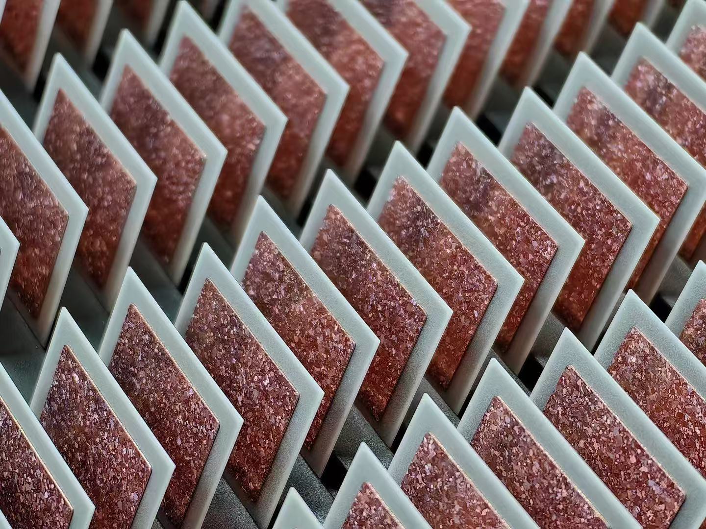
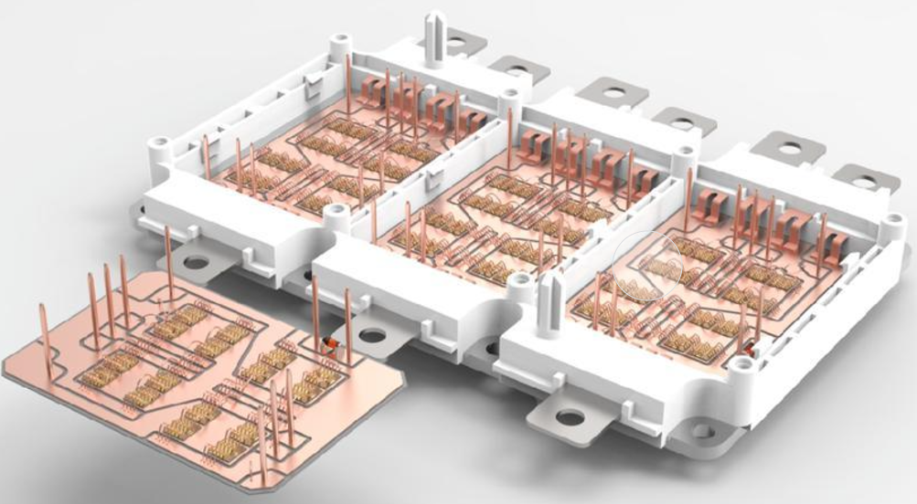
The anisotropic thermal conductivity of silicon nitride ceramics is both an advantage and a design challenge. For instance, in semiconductor power modules, substrates need high thermal conductivity in the vertical direction (from the chip to the heat sink) for efficient heat dissipation, while simultaneously requiring a thermal expansion coefficient in the horizontal direction that matches the chip material (e.g., SiC) to avoid thermal stress cracking. This contradiction forces engineers to seek a balance in material design and processing.
3.1 Grain Boundary Phase Control
The addition of sintering aids (e.g., Y₂O₃-MgO) promotes densification but forms low-thermal-conductivity grain boundary phases (e.g., silicon oxynitrides). Research shows that optimizing the sintering aid composition (e.g., using MgSiN₂ instead of MgO) can reduce the grain boundary phase content to below 5%, thereby enhancing thermal conductivity.
3.2 Oxygen Impurity Control
Lattice oxygen is a major source of phonon scattering. High-purity raw materials (oxygen content <1 wt.%) and a reducing sintering atmosphere (e.g., nitrogen-hydrogen mixed gas) can effectively reduce oxygen impurities, increasing thermal conductivity by approximately 20%.
4. Future Directions for Enhancing Thermal Conductivity
Future research directions to further improve the thermal conductivity of silicon nitride ceramics include:
Nanostructure Design: By introducing gradient grain sizes or heterogeneous interfaces, phonon transport paths can be optimized.
Composite Ceramics Development: Combining with high-thermal-conductivity materials (e.g., graphene) to break the performance limits of single-phase ceramics.
Precisely controlling the anisotropic thermal conductivity of silicon nitride ceramics is both a fundamental challenge in materials science and a key breakthrough for industrial applications. From atomic-level crystal structure design to macroscopic grain orientation control, silicon nitride ceramics are expected to approach their theoretical thermal conductivity along the c-axis, paving the way for broader applications in high-power electronics, 5G communications, electric vehicles, and beyond.