

Precision Laser Drilling Unlocks New Potential for Aluminum Nitride Ceramic Substrate
The rapid advancement of power electronics, RF communication, and photovoltaic systems demands substrate materials that can withstand extreme thermal and mechanical conditions. Aluminum Nitride (AlN) ceramics, renowned for their excellent thermal conductivity and high electrical insulation, have become the material of choice for demanding applications. However, the full potential of these advanced ceramics is only realized through precision machining techniques. Precision laser drilling has emerged as the critical enabling technology that transforms standard AlN substrates into sophisticated, multi-functional components for semiconductor, RF/microwave, and hybrid microcircuit applications.
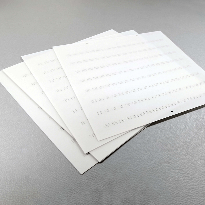
Why Precision Laser Drilling Is Essential for Advanced Ceramic Substrates
For technical buyers and engineers sourcing ceramic circuit boards and power device ceramic substrates, component integrity is non-negotiable. Traditional mechanical machining of brittle ceramics like AlN and high-purity alumina often induces micro-cracks, chipping, and residual stress. These defects compromise the very properties that make these materials valuable—high mechanical strength, thermal stability, and long-term reliability. Precision laser micromachining offers a non-contact, tool-less solution that eliminates these failure points, enabling reliable performance in mission-critical applications including IGBT ceramic substrates, microwave RF ceramic substrates, and automotive electronic ceramic substrates.
Key Advantages of Laser-Drilled Ceramic Substrates
- Unmatched Design Freedom – Create micro-vias (down to 50µm), slots, blind holes, and complex cavities for advanced thermal and electrical management in AlN ceramic circuit boards and multilayer structures.
- Preservation of Material Properties – Minimal heat-affected zone (HAZ) ensures the substrate's intrinsic high thermal conductivity, high electrical insulation, and mechanical strength are fully maintained.
- Enhanced Reliability & Production Yield – Clean, crack-free vias with smooth sidewalls ensure perfect metallization adhesion and void-free plating, critical for thick film ceramic substrates and direct bond copper (DBC) processes.
- Accelerated Development Cycles – Digital process control enables rapid iteration without hard tooling, making laser drilling ideal for custom AlN ceramic components from prototype to high-volume production.
Critical Applications Enabled by Laser-Drilled Ceramic Substrates
Next-Generation Power Modules & High-Power Devices
Thermal via arrays laser-drilled into power device ceramic substrates create direct heat paths from semiconductor dies, dramatically improving cooling in EV traction inverters, industrial motor drives, and renewable energy systems. This capability is essential for high-power device ceramic substrates where efficient thermal management directly impacts reliability and power density. Many designers now specify 96% alumina ceramic substrates for cost-sensitive applications while leveraging AlN's superior thermal conductivity for the most demanding power stages.
High-Frequency RF & Microwave Circuits
Precision via formation enables reliable ground connections, controlled impedance transmission lines, and complex multilayer interconnects. Laser-drilled microwave RF ceramic substrates deliver the dimensional accuracy and repeatability required for 5G infrastructure, aerospace radar systems, and satellite communications. The ability to create high-aspect-ratio vias in Al2O3 ceramic substrates and AlN enables compact, high-performance RF front-end modules.
Advanced Optoelectronics & Thermoelectric Modules
Micro-vias and precision cavities enhance thermal and electrical performance in LED ceramic substrates and high-power laser diode packages. For thermoelectric cooling (TEC) applications, ceramic insulating substrates for TEC and thermoelectric modules ceramic components rely on laser-drilled features to maintain electrical isolation while maximizing heat transfer—a perfect match for materials with excellent electrical insulation and good thermal conductivity.
Automotive Electronics & Harsh Environment Applications
In automotive electronic ceramic substrates, laser-drilled vias and cavities ensure reliable operation of pressure sensors, exhaust gas sensors, and power converters under extreme temperature cycling and vibration. The combination of high hardness, wear resistance, and high temperature resistance makes laser-machined ceramics indispensable for under-hood and powertrain applications.
Technical Considerations for Specifying Laser-Drilled Ceramic Substrates
Via Geometry & Aspect Ratio
Modern laser systems can achieve via diameters from 50µm to 500µm with aspect ratios up to 10:1. The choice of via size and shape depends on metallization method (thin film, thick film, or DBC) and electrical current requirements. For thick film ceramic substrates, slightly tapered vias often improve paste filling and densification during firing.
Surface Quality & Metallization Compatibility
Via wall roughness and cleanliness directly affect plating adhesion and void formation. Advanced UV and picosecond laser systems produce smooth, contamination-free surfaces ideal for subsequent metallization. This is particularly critical for ceramic circuit boards requiring high-reliability solder joints and thermal cycle performance.
Material Selection: AlN vs. Alumina
While both material families benefit from laser drilling, the choice depends on application requirements:
- Aluminum Nitride (AlN) – Thermal conductivity 170-230 W/m·K, ideal for high-power density applications where heat spreading is critical.
- 96% Alumina (Al2O3) – Thermal conductivity 24-28 W/m·K, excellent electrical insulation, cost-effective for general power and RF applications.
- High-purity Alumina (99.5%+) – Enhanced mechanical strength and dielectric properties for demanding RF/microwave circuits.
Procurement Checklist: Evaluating Laser Drilling Capability
When sourcing laser-drilled alumina ceramics or AlN substrates, assess potential suppliers against these criteria:
- Process Capability – Can they achieve your required via size, positional accuracy (±25µm or better), and aspect ratio consistently across the panel?
- Quality Assurance – What inspection methods (optical microscopy, cross-sectioning, X-ray) verify via integrity, wall quality, and absence of micro-cracks?
- Metallization Integration – Does the supplier offer or coordinate with proven via-filling and plating processes to ensure electrical continuity and thermal performance?
- Scalability & Lead Times – Can they maintain quality from prototype quantities (10-50 pieces) to high-volume production (10,000+ pieces/month)?
- Engineering Support (DFM) – Do they provide design for manufacturability feedback to optimize hole patterns, array layouts, and tolerances for cost-effective production?
Frequently Asked Questions from Technical Buyers
Q: Does laser drilling affect the thermal conductivity of the ceramic substrate?
A: Properly optimized laser drilling causes minimal damage to the surrounding material—typically a heat-affected zone of less than 5-10µm. When vias are subsequently filled with high-conductivity metals (copper, silver), they create vertical thermal paths that can actually enhance effective heat transfer through the substrate thickness.
Q: What are the cost implications for prototyping vs. mass production of alumina ceramic structural components?
A: Laser drilling is highly cost-effective for prototyping due to zero tooling costs—ideal for design validation and iterative development. For high-volume production, the combination of high yield, repeatability, and the ability to process multiple parts simultaneously often results in lower total cost compared to mechanical methods, especially for complex hole patterns and small-diameter vias.
Q: Can laser drilling be used on alumina ceramic disc and other shaped components?
A: Absolutely. Modern laser systems with autofocus and 3D positioning capabilities can process flat substrates, curved surfaces, and complex alumina ceramic structural components. This includes creating cooling channels in thick components, sensor ports in hermetic packages, and precision holes in thermoelectric modules ceramic plates.
Q: How do I select between AlN and 96% alumina for my application?
A: Consider three primary factors: power dissipation requirements, operating temperature, and budget. For applications requiring heat flux >10 W/cm², AlN's superior thermal conductivity (170-230 W/m·K) is typically justified. For lower power densities and cost-sensitive applications, 96% alumina ceramic substrates provide excellent electrical insulation and mechanical stability at a fraction of the cost. Your supplier should offer both material options and guide you based on actual thermal simulation and reliability requirements.
Conclusion: Partnering for Advanced Ceramic Performance
Precision laser drilling has evolved from a specialized capability to an essential manufacturing process for high-performance ceramic substrates. By enabling complex via patterns, cavities, and three-dimensional features, this technology allows design engineers to fully exploit the superior properties of both Aluminum Nitride and advanced alumina ceramics—excellent electrical insulation, high thermal conductivity, high mechanical strength, and proven reliability in harsh environments.
When you partner with a manufacturer like Puwei that masters both high-purity ceramic processing and precision laser micromachining, you gain more than a supplier—you gain a technical partner capable of delivering custom ceramic substrates and ceramic insulating substrates that meet the extreme demands of modern power electronics, RF/microwave systems, and optoelectronic devices. This synergy between material science and advanced fabrication is the key to building more efficient, reliable, and compact next-generation systems.
Contact our engineering team to discuss your specific requirements for laser-drilled 96 alumina ceramic substrate, AlN, or other advanced ceramic materials for semiconductor, photovoltaic, and hybrid microcircuit applications.